Design Workflows
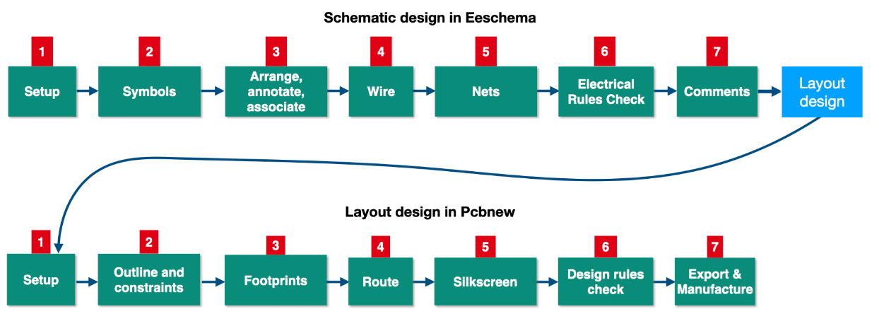
PCB design workflows systematize the transition from conceptual circuit diagrams to manufacturable boards, ensuring logical integrity, electrical compliance, and physical feasibility. Two interdependent workflows govern this process: Schematic Design (logical representation) and PCB Layout (physical realization). KiCad’s Eeschema and Pcbnew tools formalize these stages, enabling designers to iteratively refine designs while adhering to industry standards.


Schematic Design Workflow
Purpose and Scope
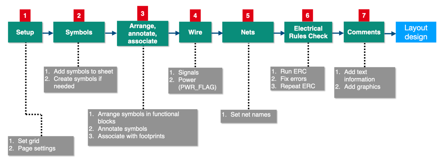
The schematic workflow defines circuit functionality through standardized symbols and interconnections, serving as the authoritative reference for layout and verification.
Key Steps
-
Project Initialization
- Create a KiCad project (.kicad_pro) with dedicated directories for schematics, libraries, and outputs.
- Configure global settings (Preferences > Symbol Libraries) to ensure access to required component repositories.
-
Component Selection
- Source symbols from KiCad’s built-in libraries (e.g.,
Device,Power) or custom libraries. - Critical components:
- Passive/Active Devices: Resistors, capacitors, ICs.
- Power Sources: Batteries, voltage regulators.
- Connectors/Interfaces: Headers, switches.
- Source symbols from KiCad’s built-in libraries (e.g.,
-
Component Placement
- Arrange symbols to reflect signal flow (e.g., power input → conditioning → load → ground).
- Align components on a 50 mil grid (View > Grid Settings) for consistency.
-
Wiring and Connectivity
- Establish electrical connections using wires (Place Wire,
W). - Define power nets (e.g.,
+3V3,GND) with global labels (Place Global Label,L). - Use power flags (Place Power Flag) to suppress ERC warnings for unconnected supplies.
- Establish electrical connections using wires (Place Wire,
-
Net Naming
- Assign descriptive net names (e.g.,
LED_ANODE,SW_SIGNAL) to simplify layout routing and debugging.
- Assign descriptive net names (e.g.,
-
Design Validation (ERC)
- Execute Electrical Rule Check (Inspect > ERC) to detect:
- Unconnected pins or conflicting outputs.
- Missing power sources or incorrect net assignments.
- Resolve errors by revising connectivity or adding suppression directives.
- Execute Electrical Rule Check (Inspect > ERC) to detect:
-
Export and Preparation for Layout
- Generate netlist (Tools > Generate Netlist) to map logical connections to physical footprints.
- Annotate components (Tools > Annotate) with unique reference designators (R1, C2).
PCB Layout Workflow
Purpose and Scope
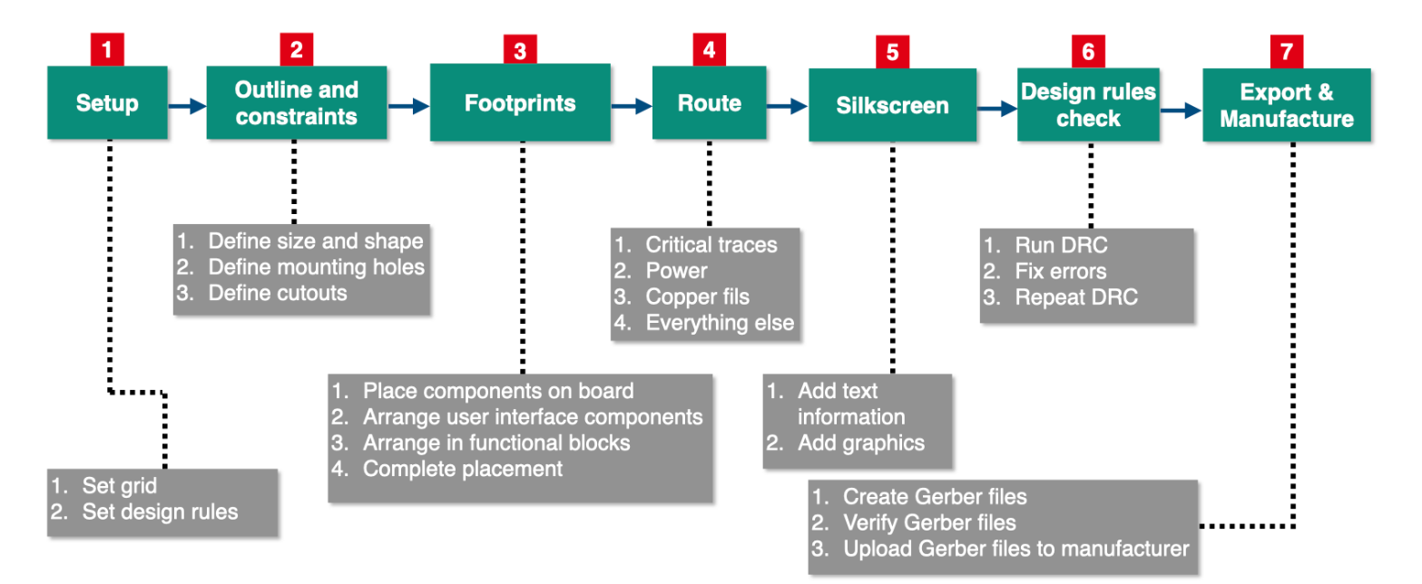
The layout workflow translates schematic logic into a physical board, balancing electrical performance, thermal management, and manufacturability.
Key Steps
-
Import Schematic Data
- Load netlist (File > Import Netlist) or synchronize via KiCad’s Schematic ↔ Layout synchronization.
- Validate footprint associations (Tools > Update PCB from Schematic).
-
Footprint Assignment
- Link schematic symbols to physical footprints (e.g.,
Resistor_SMD:R_0805,LED:LED_THT). - Verify footprint dimensions, pad sizes, and 3D models (View > 3D Viewer).
- Link schematic symbols to physical footprints (e.g.,
-
Component Placement
- Prioritize critical components (e.g., connectors, ICs) based on signal integrity or mechanical constraints.
- Group related components (e.g., power supply section, analog inputs) to minimize trace lengths.
-
Routing
- Route high-priority signals (e.g., high-speed traces, power paths) first using manual or autorouter tools.
- Define copper pours (Add Filled Zone) for power/ground planes to reduce noise and impedance.
-
Design Rule Compliance
- Configure design rules (File > Board Setup > Design Rules) for:
- Trace width (e.g., 0.3 mm for signals, 1.0 mm for power).
- Clearance (e.g., 0.2 mm between traces, 0.5 mm from board edge).
- Via styles (through-hole vs. microvia).
- Configure design rules (File > Board Setup > Design Rules) for:
-
Design Verification (DRC)
- Run Design Rule Check (Inspect > DRC) to identify:
- Short circuits, insufficient clearances, or unconnected nets.
- Footprint overlaps or misplaced vias.
- Iterate placement/routing until all violations are resolved.
- Run Design Rule Check (Inspect > DRC) to identify:
-
Manufacturing Preparation
- Generate Gerber files (File > Fabrication Outputs > Gerber) for each layer (copper, solder mask, silkscreen).
- Export drill files (File > Fabrication Outputs > Drill Files) in Excellon format.
- Validate outputs using Gerber viewers (e.g., KiCad’s GerbView) or manufacturer design rule checks.
Iterative Workflow Dynamics
Design workflows are inherently cyclical, requiring revisions to earlier stages based on validation outcomes:
- Schematic Revisions: ERC errors (e.g., unpowered nets) may necessitate revisiting component placement or wiring.
- Layout Revisions: DRC failures (e.g., trace spacing violations) may require footprint rearrangement or schematic net adjustments.
- Cross-Workflow Synchronization: Changes in schematic symbols (e.g., pin swaps) propagate to layout via netlist re-import.
Workflow Simplification Strategy
For Beginners
- Linear Progression: Execute workflows sequentially (schematic → layout) to build foundational skills.
- Guided Validation: Rely on ERC/DRC tools to flag errors without premature optimization.
For Advanced Users
- Concurrent Refinement: Modify schematics and layouts in tandem to address signal integrity or EMI constraints.
- Design Reuse: Leverage hierarchical sheets and custom design rules for multi-board or high-density projects.
Expected Competencies
By mastering these workflows, designers will:
- Navigate KiCad Tools Efficiently: Proficiently utilize Eeschema and Pcbnew for end-to-end PCB development.
- Implement Robust Validation: Resolve ERC/DRC issues through systematic debugging.
- Optimize for Manufacturability: Generate industry-standard outputs (Gerber, drill files) compatible with PCB fabrication.
Transition to Advanced Design
The structured workflows provide a foundation for tackling complex projects, such as:
- High-Speed Digital Design: Impedance-controlled routing, length matching.
- Mixed-Signal Layout: Ground partitioning, noise isolation.
- Thermal Management: Heat sink integration, thermal relief patterns.
This methodological rigor ensures designs meet functional, reliability, and production requirements at scale.